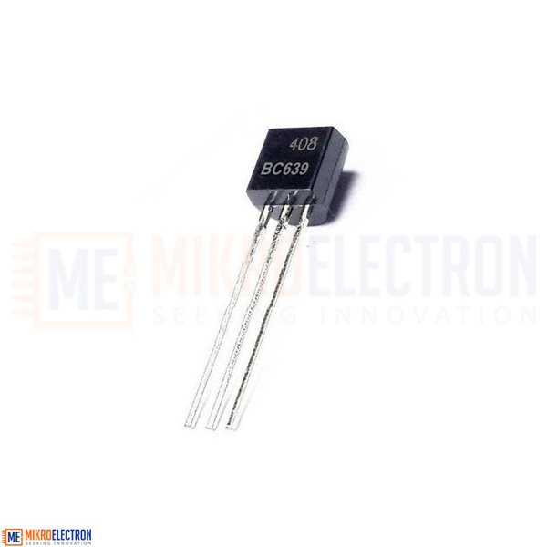
BC639 General Purpose NPN Transistor

Description:
The BC639 is an NPN Transistor in a TO-92 package which has a VCE of 100V and a continuous collector current of 1A. With this characteristic and 1W total power dissipation, this transistor can be used in moderately high voltage switching applications.
BC639 Pinout Configuration
|
Pin Number |
Pin Name |
Description |
|
1 |
Emitter |
Electrons emitted from the emitter
into the first PN junction |
|
2 |
Collector |
Electrons Emitted from Emitter
Collected by the Collector |
|
3 |
Base |
Controls the biasing of the
transistor |
General Description of BC639 Transistor
The BC639 transistor is a very versatile transistor that can be used in many different applications. This transistor can be used to switch moderately high voltage devices, like a small DC-DC converter, or a pre or mid amplifier stage of a power amplifier, generally, a power amplifier uses something like 60 to 120V DC this transistor can be useful for this kind of applications. The component is cheap and easy to work with so it is best suited when choosing a random switching device. When this transistor is in a biased condition, then it can allow a maximum current of 1A across CE(Collector-Emitter) Junction, this state of the transistor is called the saturation state, and driving a load that consumes more current than 1A may damage the device permanently, also during the design process, you need to be aware that the maximum dissipation of this device is 1W, power more than that can damage the device.
As you already may know, a transistor is a current-controlled device so when the base current is removed the transistor becomes fully off, in this stage the transistor is working in its cut-off region/cut-off state and no current flows through the C-E junction. The BC639 transistor has a gain of 40 to 160, this value determines the amplification capacity of the transistor, the peak current that can be flown through this transistor is 1.5A which combined with the gain value makes this transistor a perfect choice for moderate-high voltage application.
Under normal circumstances and without external influence, the base of an NPN transistor will be 0V. As we all know, based on the working principle of an NPN transistor; having 0 voltage at the base puts an NPN transistor in a high resistance state. By characteristic a small amount of current needs to flow out of the base of the transistor to completely turn on the device, for this device you can see, in order to flow 1000mA of current through the collector to emitter, 50mA of current needed to flow through the base of the transistor.
Applications:
Simple switching applications
Microphone preamplifiers
Lighting systems
Relay drivers
Audio Amplifiers
Signal Amplifiers
Note:
Complete Technical Details can be found in the BC639 datasheet given at the end of this page.
Features:
- Bi-Polar NPN, high voltage Transistor
- DC Current Gain (hFE) is 160 maximum
- Continuous Collector current (IC) is 1A
- Emitter Base Voltage (VBE) is 5V
- Base Current (IB) is 100mA maximum
- Maximum Collector-Base Voltage |Vcb|: 50 V
- Collector Dissipation: 1 W
- Transition Frequency:100 MHz
- Collector Capacitance 20pF
- Operating Junction Temperature Max (Tj): 150 °C
- Available in TO-92 Package
Kit include:
1 x BC639 General Purpose NPN Transistor
Related Products
subscribe to our weekly newsletter
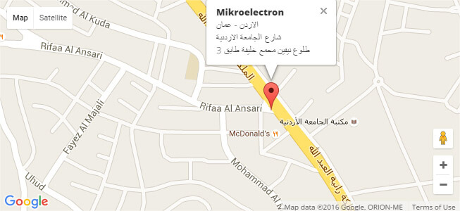
We are an online electronics store based in Jordan-Amman. The products we sell ranges from electronic products to modules and much more.
- AMMAN, Jordan. University Street, Khalifa Building 3rd floor
- Mobile: +962 7900 621 96, +962 65344772, +9627 8877 5522
- Phone: +962 6 5344772
- Fax: +96265344778
- Email: info@mikroelectron.com

2024 © Mikroelectron. ALL Rights Reserved. | Distributor Area
Made With By Tashfier.